
Activities
Flexible Electronics
Smart Sensors
Microelectrodes Arrays
Polysilicon TFT
O-tft (pentacene)
Microcrystalline Silicon TFT
Silicon Nanowires Growth
Device Physics
Flexible Electronics
Flexible microelectronics offers many advantages over rigid backplane, such as lower production cost, lightness, robustness and adaptability to non planar surface. The recent development of electronics on plastic allows the conception of new applications in different areas of consumer electronics, such as active matrix liquid crystal displays, flexible displays, bio-medical devices, automotive applications, sensors, etc. The polycrystalline silicon TFTs have been recently investigated for the realization of electronic circuitry on flexible substrate in consideration with its good integration capability respect to standard c-Si CMOS technology. To date polysilicon TFTs fabrication process is becoming totally compatible with new plastic materials that have higher glass transition temperatures, low surface roughness and low Coefficient of Thermal Expansion. Our research activities fully take into account these technological approaches, allowing the fabrication of flexible array of poly-Si TFTs, bendable humidity sensors and other gas sensors. |
 |
Smart Sensors
Flexible sensors are gaining increasing interest in a number of applications, including biomedical, food control, domotics and robotics, having very light weight, robustness and low cost. In order to improve signal-to-noise ratio, integration of readout electronics is crucial and several technologies are available for the fabrication of thin film transistor (TFTs) based circuits on flexible substrates. Among these technologies, the low temperature polycrystalline silicon (LTPS) is particularly attractive, since LTPS TFTs show excellent electrical characteristics, good stability and offer the possibility to exploit CMOS architectures.
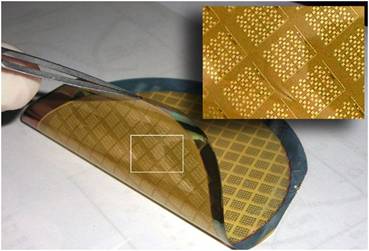
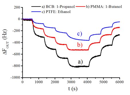
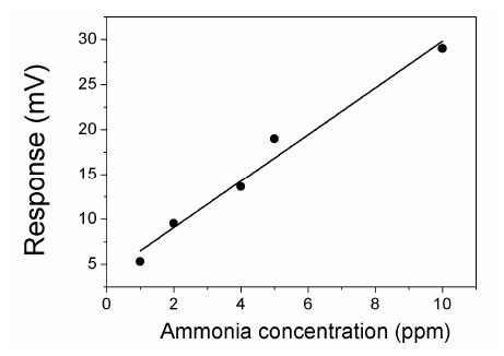
LTPS TFTs based flexible electronics can provide a proper sensor signal amplification and conditioning, but in order to further reduce the fabrication cost, minimize the device dimensions and maintaining a high degree of system mechanical flexibility, read-out circuit interfaces must be integrated on flexible substrate together with sensors. We fabricated both resistive and capacitive flexible sensors integrated with read-out interface based on LTPS TFTs. With this technology, we could detect volatile organic compounds (VOCs), (e.g. Ethanol, Propanol, Methanol, Lactic Acid, etc.), gases (e.g. NH3) and humidity.
 |
 |
 |
 |
The interaction of humanoid robots with different and complex environments demands the implementation of sophisticated sensory capabilities. In particular, the development of tactile sensors is one of the key technical challenges in advanced robotics. Among different touch sensing technologies, piezoelectric flexible pressure sensors, integrated with polysilicon electronics, are particularly suitable for the definition of a so called artificial skin, since this technological platform can be tailored on non-conventional surfaces and miniaturized for the integration of the sensors into some critical areas such as robot fingertips.
We developed a novel technique, in collaboration with IIT in Genoa, for the fabrication of smart ultra-thin pressure sensors based on polysilicon TFT elelctronics.
 |
 |
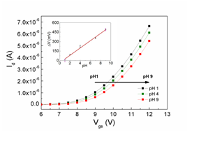
Ultra-flexible pH sensors by IMM-CNR Rome Unit
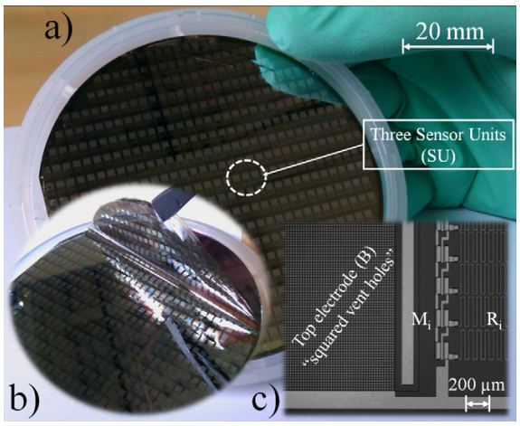
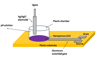
We developed a fully flexible pH sensor based on an extended gate architecture constituted by a poly-Si TFT integrated on ultra-flexible polyimide layer and a sensing layer formed by ZnO nanowall growth by hydrothermal technique. The pH sensor showed an ideal Nernstian response (59 mV/pH), suggesting that the reported technology can be applied for the fabrication of flexible biosensors.
 |
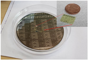 |
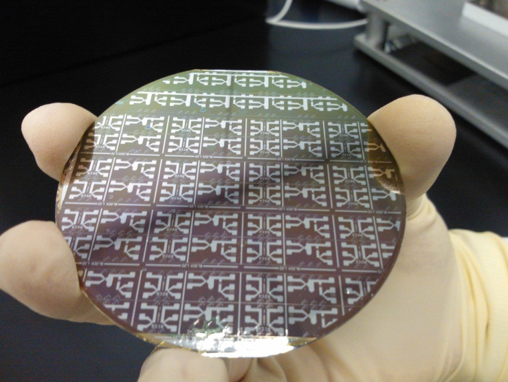
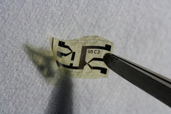
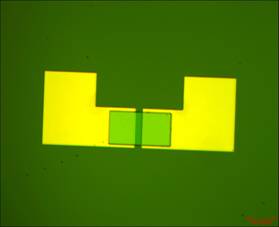
| Schematic of the flexible pH sensor, based on an extended gate poly-silicon TFT integrated with a ZnO nanostructured membrane | An image of the devices on the wafer (in the centre some structures are already detached); in the inset the devices before the growth of ZnO nanowalls |
 |
|
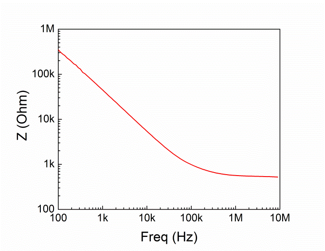
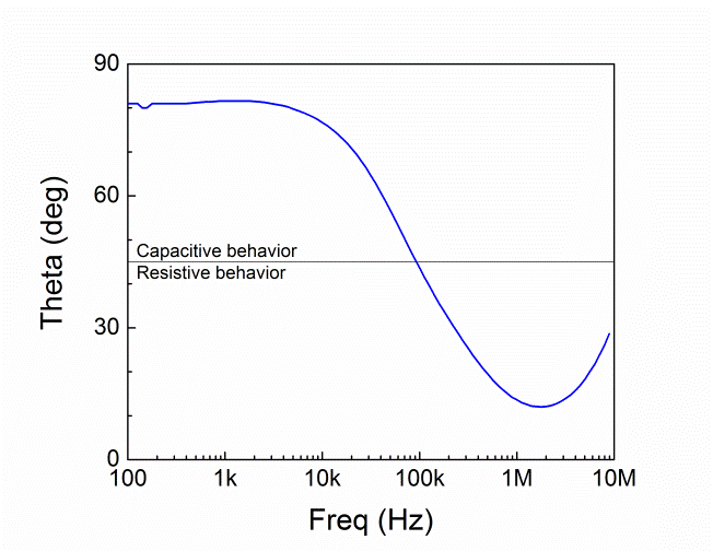
Microelectrodes Arrays 
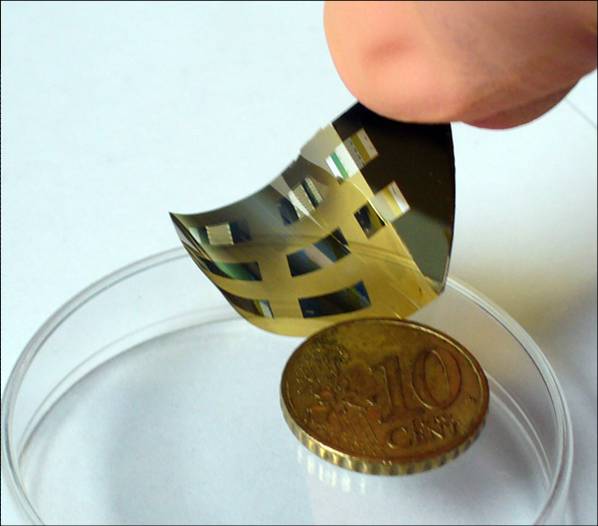
| Micro and nano-electrodes arrays fabricated on flexible and extremely thin substrates are devices that can be successfully employed in different fields such as smart sensing, neural signal recording, microstimulation, etc. Among microsystems targeted to biomedical applications, chronically implantable interfaces with the nervous tissue are increasingly considered for the definition of closed-loop Brain-Computer Interfaces. These kind of devices can enhance the control of symptoms of several neurological disorders and improve the final outcome of neuro-rehabilitation. Microelectrodes are wires made of a conducting metal, such as platinum, gold, tungsten, iridium, or stainless steel, that are coated with a non-cytotoxic insulator material. The tip of the wire is not insulated and can receive electrical signals from the surrounding neurons. Microelectrodes can be arranged in arrays to access the large numbers of neurons. These devices can be used for both in vitro and in vivo studies. |
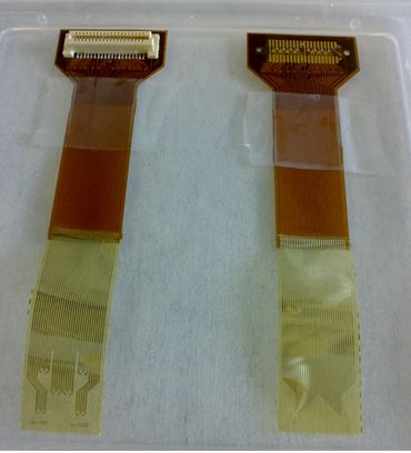 |
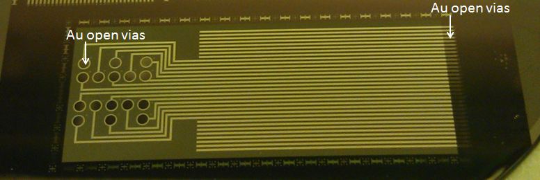
| We can realize high conformable and ultra-thin flexible grids with different metals (Au, Ti, Ag, Pt, PEDOT, etc.). The exposed metal areas can range from 3 mm2 to 2500 um2. We can interconnect the ultra-thin microelectrodes array with standard PCB made in kapton, exploiting a Flex-on-Flex (FOF) assembly technique by a reflow soldering machine. We also test in vitro the devices measuring the impedance magnitude and phase of recording channel as a function of frequency. |
 |
 |
Polysilicon TFT
| Design and fabrication of high-performance polycrystalline silicon thin-film transistors are the primary research activity of ALADIN group. This research activity has been supported, in the years, by different collaborations with companies like Philips, ST-Microelectronics, THALES and European projects as ECAM III and FlexiDis. In our labs, the poly-Si TFTs fabrication process is carried out in all its technological steps: thin film deposition (dielectric layers and semiconducting layers) using PECVD and ECR-PECVD, polysilicon crystallization by excimer laser annealing, photolithographic pattern definition and contacts metallization. In order to better comprehend the electrical mechanisms inside the transistor and in order to improve device performances we investigate different TFTs architectures. We develop several strategies with the purpose of increasing the grain size of the polysilicon active layer working on both the precursor amorphous silicon layer and the laser beam profile. | 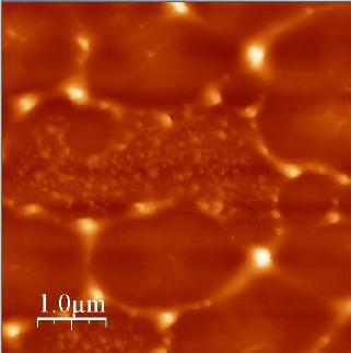 |
O-tft (pentacene)
The new opportunities that the use of organic semiconductors offer to device fabrication in the field of large area, low-cost and flexible electronics, have recently increased the research efforts on these materials. Recent results have shown that devices based on some organic semiconductor can be easily compared with those based amorphous silicon. Indeed, the performance obtained with pentacene-based organic thin film transistors (OTFTs) make possible that OTFTs are used as drivers of organic light emitting diodes in high-resolution active matrix displays. Today pentacene TFTs can be fabricated using inorganic and organic materials as substrates. The applications in microelectronics require very reliable devices with relative good on current stability: infact today, one of the main challenges, related to the processing of organic semiconductor, is the possibility to find a protective coating enabling patterning of the active layer as well as preventing aging effects caused by air and humidity. The use of conventional optical lithography to pattern pentacene active layers has been already demonstrated, in combination with different passivation film, including PVA, parylene.
 |
 |
Microcrystalline Silicon TFT
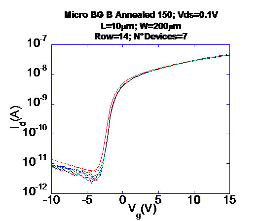
In view of applying the ECR-PECVD oxide, developed by the ALADIN group, to microcrystalline silicon TFTs a series of experiments have been scheduled jointly with CNRS Ecole Polytechnique. This work was focused on the realization of three different microcrystalline silicon TFTs structures on two kind of substrates: Corning Glass and thermally oxidized c-Si wafer. In order to investigate the active layer properties, the different TFTs structures were projected: staggered-electrode top and bottom gate, and coplanar-electrode top gate. Several wafers were fabricated and characterized in order to analyze the TFTs electrical stability and their electrical uniformity inside the wafers and from wafer to wafer. These results were compared with similar devices fabricated at University of Stuttgart. Moreover the device performances were studied together with standard amorphous silicon TFTs. |
 |
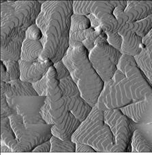
Silicon Nanowires Growth
Nanowires (NWs) are going to become the building blocks of several kinds of future devices, and for this reason they are presently among the most pursued topics in solid-state physics. This newly started activity on the growth of silicon nanowires has the objective to develop growth protocols compatible with low-temperature device processes and able to produce NWs with excellent electronic properties. NWs are generally grown after the vapour–liquid–solid model, by using a metal nanoparticle (NP), the catalyst, that induces and dictates the growth. The NP is then found at the free end of the NW. The most commonly used metal is gold. However, the catalyst may diffuse into the wires inducing unwished changes of the NW electronic properties. In particular, Au should be avoided when growing Si NWs or integrating III-V NWs with Si substrates, being Au a very efficient carrier trap in Si. Growths at low temperatures with catalysts alternative to gold or without the use of any external catalyst are then the first practical goals to achieve. |
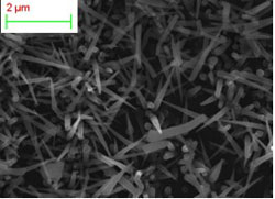 |
Preliminary results are shown in the figure that shows a SEM image of Si nanowires grown without catalyst at 430 °C, a temperature considerably lower than those indicated in literature for catalyst-free Si NWs.
Device Physics
The physics underlying the devices behaviour is investigated by using the 2D and 3D numerical simulation program DESSIS. Transport in amorphous and poly-crystalline silicon can be simulated by using the effective medium approach, which introduce a density of acceptor and donor states, exponentially distributed respectively from conduction and valence band, throughout the material energy gap. Moreover, the effect of interface states between semiconductor/oxide and semiconductor/ semiconductor interfaces can be simulated. This approach has been used also for the simulations of organic based (pentacene) devices.
The simulation software allow the use of different models for the semiconductor equations: drift-diffusion, thermodynamic model (which accounts for the device temperature field), hydrodynamic model (which accounts for the energy exchange between carriers and lattice). Among the physical mechanisms that can be included in the simulations we note: impact ionization mechanisms (needed for output characteristics simulation), bulk and interface traps models, generation-recombination models.
Several topics have been investigated:
Transport and reliability of polycrystalline silicon TFTs with advanced drain architecture
Transport in presence of grain boundaries
Self heating effects
Floating Body Effects
Short Channel Effects
Negative Bias – Temperature Instabilities (NBTI)
Aging and Hysteretic effects in OTFT
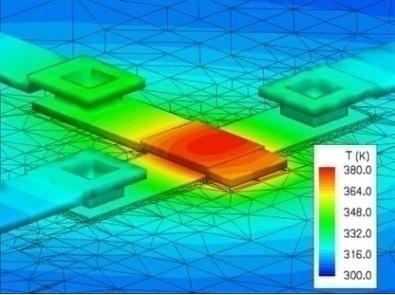
Temperature distribution inside the polysilicon active layer of a TFT biased in the self-heating regime
abrupt
s = 60 nm
s = 100 nm
s = 200 nm
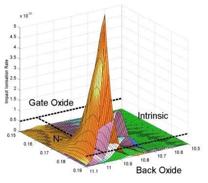
Impact ionization rate at the drain junction of a polysilicon TFT for different values of the lateral penetration of the doping.